|
|
The
increasing need to achieve production capability on 0.4 mm pitch technologies
and beyond with high assembly yields and improved solder joint reliability
is driving further changes in surface finishes. This drive for change
is also met by environmental challenges, largely represented by the elimination
of lead, and is additionally coerced by pressures to drive down costs.
As a consequence, a new generation of immersion metal finishes is pervading
the electronics industry. These finishes include silver and tin variants,
which have the particular advantage of common and/or compatible base metallurgies
with the solders and pastes applied during assembly. This benefit extends
not only to lead containing (63/37) products but also to lead-free commodity
or solder alloys.
The current issues with interfacial stress fractures affecting array components,
mainly BGAs (ball grid array) but also QFPs (quad flat pack), have been
widely reported. These have served not only to fuel the quest for alternatives
to nickel/gold plating, but have also heightened the awareness of the
critical performance and reliability questions associated with surface
finishes.
 |
|
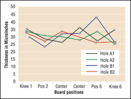
Tin plating thickness distribution - (9.75:1) high aspect ratio holes. |
Such
change is needed, but the engineering support required for testing and
commissioning new materials presents a serious but mandatory burden on
the OEM and EMS industries. However, this is only one aspect of the impact
of the progressive change in surface finishing. The integration of such
new processes within the PWB fabrication sector also presents some significant
challenges. The board maker has to be able to install the process with
minimal cost impact to the board. The new process has to be compatible
with existing manufacturing procedures, or they have to be readily adjustable
to accommodate the new system. The process and procedures have to be quickly
optimized so that the finish can be applied consistently and reliably.
The product has to meet the increasingly stringent quality assurance standards,
and the appropriate methodologies and metrics have to be put in place.
The new process has to run consistently, reliably and measurably. With
any new manufacturing technology within the PWB industry, one other important
challenge is also leveled at the industry as a whole. How can the industry
and its consortia of task forces, study groups and committees come to
terms with the benchmarking needed? How can the specialty chemical vendor,
the board fabricator, the assembler and the OEM understand the impact
of the new process? How can they work in synergy to capture the benefits,
guard against the threats and complete a win/win selection procedure?
These are some of the challenges that the flat solderable immersion tin
finish technology has had to address.
 |
Challenges
for the Immersion Tin Finish
The benefits and challenges of planar tin finishes have been reported.
The impact on the OEM and assembler is critical. The tin system described
in this article was first introduced into the European market during late
1993 and was more latterly promoted into the North American market from
1997. When installing this type of process, some of the key challenges
that need to be confronted and addressed by a board fabricator are as
follows:
1. Should the system be installed in a dip or conveyor system, particularly
for high aspect ratio holes or thick boards?
2. How well can the process be controlled to give a consistently solderable
finish?
3. What are the response variables for the parameters used to drive the
process?
4. What are the expected plating distribution profiles?
5. How can the deposit thickness be quickly and accurately measured?
6. Is the deposit compatible with or can it be damaged by an electrical
test?
7. Can effective supply specifications and quality metrics be agreed between
the PWB fabricator and the customer?
8. Can the process be continuously used for minimal waste disposal?
9. How well does the new process integrate into the manufacturing sequence?
10. What is the impact on the PWB materials e.g. LPSM, legend, hole-plug,
etc?
11. How clean is the surface in terms of ionics, and how can rinsing be
optimized?
12. Can different types of pretreatment be applied with success?
13. Do good rework procedures exist and what is the impact on the copper
thickness particularly on the hole-wall?
Dip
or Conveyor Processing?
A frequent question in the early days of the process was the net impact
of the process type. The following generalized test data resulted from
the use of the process shown in Table I, which shows a typical dip process
sequence. When installing dip-immersion tin systems, emphasis needs to
be placed on the equipment design, particularly the materials of construction,
filtration and circulation of the tin tank. Rinse stages, water flow rates,
quality and temperature are key requirements, as is the need to get completely
dry holes, which is best achieved using a horizontal dryer.
A
flooded immersion conveyor sequence is similar, but the immersion time
in the tin would be reduced to approximately 6 min and the pretreatment
and rinse times would also be reduced. The conveyor process for regenerable
systems also uses a nitrogen blanket to prevent oxidation of the tin and
to ensure a clean running system with no precipitation.
The conveyor process is used in volume production applications to plate
holes down to 0.25-0.3 mm (0.010-0.012 inch) diameter in thinner boards,
and down to 0.5 mm (0.020 inch) in thicker 5.5-6.0 mm (0.216-0.236 inch)
boards. This gives an aspect ratio capability down to 10-12:1. Problems
have only arisen if the high aspect ratio holes are partially blocked
or plugged at one end. These are more critical and need thorough wetting-out
and more efficient cleaning and micro-etching. As would be expected in
these cases, LPSM (liquid photoimagable solder mask) development and rinsing
are also critical. Residual oxide in buried holes can be difficult to
clean and panels may have to be double passed to get full plating. A good
guide is to look at the copper appearance on incoming product. This should
be shiny, which normally ensures good small-hole production plating capability
of the tin.
One
of the challenges to conveyor systems is the ability to deal with thicker
back plane boards, which can be more effectively handled in dip processes.
A small controlled study has shown that on 9.75:1 aspect ratio holes (0.041-inch
holes in 0.400-inch-thick boards) the average plated hole thickness in
four test coupons was 30.2 microinches.
The results are shown in Figure 1, and the boards were vertically dip
plated at 150F for 8 min. The distribution was good, and the lowest thickness
figures of 23-25 microinches were not found in the centers of the holes.
While no thin areas of plating were detected, the measurement technique
for holes was more difficult and required a specially calibrated XRF and
SEM cross-section comparison.
  |
Plating
Thickness and its Measurement
The X-ray fluorescence technique is the fastest and most reliable non-destructive
method to determine immersion tin thickness. However, the method only
detects the presence of tin and derives a coating thickness based on the
mass of tin present in a given area of the circuit board. The XRF sees
the coating as if it were a single layer of pure tin with a theoretical
density of 7.29 g/cm3. The problem is that proprietary immersion tin deposits
have unique compositions, which may incorporate a significant amount of
copper, organic material and/or other trace metals. This can be verified
by using Scanning Auger Microanalysis. Consequently, the real density
of tin in the finished deposit can be much less than 7.29 g/cm3 and, in
some cases, may be close to 50% of the theoretical value.
Hence, to avoid major noise factors, which can skew the measurements,
the method to be applied is critical. This is vital when the thickness
is being written into OEM specs.
Solderability
Control
It may seem obvious, but the essential requirement of a solderable tin
finish is its good "solderability." The question immediately
arises as to how this is measured, benchmarked and a specification agreed
between the supplier (PWB fabricator) and the customer (PWB assembler).
A directly related question becomes which method of stress testing should
be applied as a performance test to simulate long-term storage and multiple
heat cycle capability. If a meniscograph is used, the selection of test
coupons is important to minimize any noise factors and give the best gage
capability. Several approaches for assessing solderability exist, and
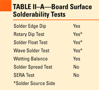
a list is shown in Tables IIA and B, including reference in the IPC Joint
Standard 003A. The question is what should be the preferred approach for
a finish?
 |
|
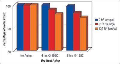
Solderabiltiy by hole filling after 155C dry heat aging for 4-8 hr. typical results. |
One
particular method, which has evolved for immersion tin, involves the use
of dry heat aging at 155C for 4-8 hr. It is interesting to note that the
oxidation rate of tin and the growth rate of copper/tin intermetallic
are similar for all tin and tin lead alloys at this temperature. The plated
samples can be heated for about 4, 6, and 8 hr and the solderability assessed
by various methods. It has been found that a hole-fill test (using J-Std
003 acceptance criteria) gives an excellent indication of solderability.
The test coupons should have a large number of 0.025-inch diameter holes
to enable a valid statistical count and, after baking, they can be solder-floated
or wave soldered and assessed. The design and build of the coupons should
be agreed with the vendor, as well as the minimum hole-fill requirements.
Oven temperature control is critical to accurate readings, and hot spots
must be avoided. A multiple thermocouple/chart recorder should be used
to check accuracy and spread, and a fan-assisted oven will give the best
temperature distribution. Based on this testing, a minimum hole fill of
95% after a 4-hr test should be expected to give good solderability for
most applications. However, the product should still give >95% hole
fill after a 6-hour bake at 155C (See Fig. 2).
Damp
Heat Testing
Although the J-Std 003 and Mil specs call out for steam aging testing
for solderability of tin and tin lead finishes, this test is not appropriate
for non-fused finishes such as OSPs (organic solderability preservative)
and immersion tin. While some data has been published for various immersion
tins and other finishes, the results are somewhat variable and inconsistent.
This view is shared by the IPC Task force, which is currently working
on solderability testing for alternate solderable finishes. A large study
was underway looking at a wide range of stress testing conditions, including
a temperature range of 50-95C; relative humidity of 30-95%; and stress
time of 8-1,000 hr. Testing has been made using meniscograph, SERA (selective
electrochemical reduction analysis) and visual determination.
 |
|
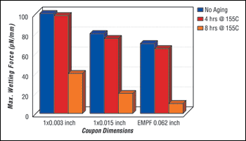
Meniscograph solderability: typical results after 155C dry heat aging using various coupons. |
The
finishes tested include two immersion tins; immersion silver; OSP; nickel-gold;
bare copper; and fused 63/37 tin-lead as the benchmark. The purpose of
the IPC testing is to determine a relationship between environmental stress
conditions such as temperature, moisture and time, and the solderability
of alternate PWB surface finishes. From this work, the objective is to
develop a model that can be used to 1) Determine screening test conditions
to assess board solderability during production; 2) Evaluate solderability
process capability for a given surface finish; and 3) Evaluate potential
new alternative surface finishes and compare solderability performance
to current finishes.
Based on extensive work with the described finish, the solderability results
after 85C/85% RH testing can give an excellent guide to performance after
storage under higher levels of humidity. Again, a hole-fill test or a
meniscograph test can be used. The problem with this type of damp heat
aging is the test duration from 1-7 days, which is not a real time test.
This makes the 4-6 hr dry heat test a more viable proposition. Some details
of meniscograph testing and hole-fill testing after accelerated aging
using dry heat and damp heat stressing techniques are shown in Figures
3a and 3b.
The other important factor is having an awareness of the impact of the
wetting balance (meniscograph) methodology, which can give some variability
on testing. Figure 3b shows the impact of the type of testing coupons
applied.
The biggest practical problem confronting the use of solderability stress
testing, as applied by the PWB fabricator as a measure of performance,
is the time factor. Any stress test (accelerated-aging test) takes a substantial
amount of time.
 |
|
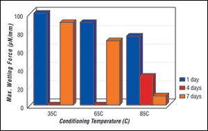
Meniscograph solderability after damp heat aging vs. temperature for 7 days. |
This
is a major concern to the fabricator who can process a lot of product
during a 6-hr test period. There is no "quick fix" stress test
to get around this problem. Hence, there has to be a good understanding
of process parameters and process variables and their long-term influence
on solderability performance.
The accent should be on "trend monitoring" and not on just spot-checking.
SERA
Testing
Other test methods have been proposed to try and give a more real time
test, including SERA (selective electrochemical reduction analysis). SERA
can be applied to assess the chemical constitution not only of the surface
features but also of the through-holes.
Two test approaches are required to get a complete picture of the finish.
The first approach is the non-destructive reduction test, which can assess
the presence and amount or surface oxides, SnO and SnO2. This uses a borate
buffer solution in the apparatus. The second involves the use of a destructive
oxidation test using a hydrochloric electrolyte that strips selectively
through the layers of pure tin and Cu6Sn5 and Cu3Sn intermetallics. A
measurement of the free surface tin will give an indication of solderability.
Unfortunately, the test may not effectively predict the change in solderability
due to thermal stress as the growth rates of intermetallic (which reduce
the available free tin for soldering) will vary with different proprietary
tin finishes. The various co-deposition techniques and boundary layers
that are formed will vary between the processes and will ultimately distinguish
the absolute performance of the tin finish. Therefore, there is a strong
argument that a stress test is still needed to validate the finish.
Process
Variables Influencing Performance
Several different immersion tin technologies are available, some based
on methane sulfonic acid and others based on sulfate, chloride and fluoborate
chemistries. In addition, various organic additives can be used to accentuate
performance and refine the characteristics of the deposit to eliminate
porosity and increase polygonization to prevent whiskering. Because of
the diversity within the range of immersion tin systems on the market,
it is beyond the scope of this paper to even attempt to characterize all
the products. However, it is clear that process performance, and hence
the nature of the plated deposit, can and will vary with changes in the
constitution of the plating bath. The tin concentration, thiourea concentration,
copper level, organic level and total acidity are all likely to impact
the thickness, constitution and solderability of the finish. It is important
that these factors are understood and controlled to the levels specified
by the vendor.
It is also important to realize that many tin processes are limited by
copper buildup, and the baths have to be disposed of and renewed. Other
systems are much more tolerant to copper in solution and are capable of
regeneration. This type of bath gives a more dynamic state of equilibrium,
better use of process chemistry and reduced environmental discharges.
The copper is self-limited by drag-out to around 5-6 g/liter in conveyor
mode or 3-5 g/liter in dip. The same organic by-products of the bath are
removed by allowing them to settle at room temperature. Hence, establishing
and controlling the correct decant frequency is important. This can be
tracked by the dry heat aging (hole fill) solderability test, and a typical
bath will be able to process some 80-120 sq ft/gal between procedures.
Two tin baths will be required for continuous operation and should be
factored into the installation.
Process
Integration
A major factor for the PWB fabricator is the actual integration of the
tin process into the manufacturing sequence. Tin can be applied in panel
form (dip or conveyor) prior to other finishing operations. Alternatively,
it can be applied to finished circuits, if the conveyor handling system
will deal with the size of parts in question. The latter will minimize
any downstream interaction of the plated circuit with heat cycles from
legend application, thermal hole or de-warp bake. However, it will expose
all the external board materials to the acid tin solution, which is running
at 150 -160F for 6 - 8 min. This may impact the nomenclature ink or may
result in residual chemistry in partially plugged holes. Trapped solution
can leach out and cause a corrosion problem after the circuits are packed
and dispatched.
The most practical approach is to process the boards in panel form, which
will enable the use of both dip and conveyor equipment. There are several
key issues to address. First, will the panels be electrically tested?
Second, what is the approach for hole plugging? If this is to be carried
out after plating (to facilitate easier rinsing and drying) then it makes
no sense to subject the plated panels to an additional heat cycle. The
recommended approach is to use a UV curable plug, applied after immersion
tin, which will have minimal impact on the performance of the finish.
The same is true of an extensive de-warp bake, which should also be avoided
after tin plating, or indeed after any other non-HASL (hot-air solder
leveling) final finish is applied.
When dealing with gold tabs or fingers, should this operation be carried
out before or after tin plating? If gold is done first, then the best
approach is to use a peelable resist to cover the precious metal to avoid
any graying of the gold. If the gold is done last, then the tin finish
needs to be well protected from the vapors or wicking effect of the gold
solution, which can cause localized solderability problems or even some
accelerated corrosion of the tin or underlying copper. Another concern
is the impact of the protective resist covering the tin in terms of tape
residues or a stripping process to remove dry film. As a general consequence,
the "tin last" operation is preferred and is generally more
practical and cost effective.
 |
Electrical
Test
A question frequently arising is whether to electrically test before or
after the tin, and what is the impact of any probe-induced damage on the
integrity of the layer. Experience working with the flat solderable tin
system has shown that the product tests well on conventional bed of nails
modules. The optimum tip style is rounded or bullet tips, since no problems
were encountered with scratching or indentations. The tin finish in question,
although apparently soft on the surface, has a fairly hard undercoat and
is difficult to scratch to reveal any copper underneath.
 |
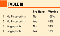
Solderability
Solderability was performed by immersing the samples in Kester 951 flux
and then laying the samples on the surface of the molten solder in the
460F solder pot. The measurements reflect the amount of SMD (surface mount
device) pads that wetted. The bake was at 300F for 4 hr, which was performed
after applying various fingerprints from three different individuals.
The results are in Table III.
Interaction
and Compatibility of LPSM
Perhaps the most important consideration from a process integration standpoint
is the question of LPSM compatibility and interactivity. This is probably
true of other surface finishes like electroless nickel/immersion gold
and HASL, and is equally important for tin. While the body of the LPSM
is generally resilient, the photo-defined edges, which may have areas
of leaching and/or undercut (from the expose and develop operation) are
often susceptible to attack. Poor or inadequate pre-cleaning prior to
LPSM application can exacerbate this attack, and excessive cleaning/micro-etching
after final cure can also be an issue. The immersion tin processes operate
at relatively high temperatures, up to 160F (some products for up to 20
min). The process used for the tests has a nominal dwell time of 8 min
in dip. Some masks, especially the newer generation of acrylic-epoxy technologies,
are hydrophilic and can quickly pick up moisture and other liquid-borne
material resulting in increased ionics. This necessitates thorough rinsing
and, in some cases, additional curing or post cleaning.
 |
A
series of extensive DOE based studies have been performed on a range of
commonly available LPSMs looking at the impact of the process.
The first DOE study (see Table IV) focused on baselining the products,
looking at ionics build up and also measuring the effects of different
pre-cleaning systems and UV bumping. Mask integrity was measured by applying
both the ASTM crosshatch scratch test and also a tape edge-lifting test.
Ionics were measured using an Omegameter 600SMD heated unit operating
at a nominal of 105F.
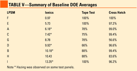
For each mask group of the 9 tested, a full factorial DOE was applied and this is shown in Table IV. The DOE involved the preparation of a total of 176 panels (not all groups had special hardeners available). The DOE response variables which were tested, were as follows:
- Ionic Contamination µg/inch2 NaCl equivalent (Omega meter 600SMD)
- Adhesion Tape Test (1=Pass or 0=Fail)
- Adhesion
ASTM D3359-95 (5B = best; 0B = worst)
The results recorded showed a wide range of responses for the different masks. These are briefly summarized in Tables V and VI, where Table V shows the average responses for all the test coupons. This gives a good relative idea of overall performance. The average results give a clear indication that two of the LPSMs tested (E and F) gave good ionics and mask integrity across a wide range of conditions.
Discussion
of Ionics
Mask F was a 100% epoxy solvent developable mask and was not particularly
influenced by any of the main factors. However, the next three masks in
Table V, E, A and C, show that the ionic levels were improved significantly
by the application of a post clean (Alpha CE2263) and to a lesser extent
by the UV bump. These masks were all aqueous developed acrylic/epoxy types.
Whereas ionics reduction in the next group of masks, G, D, B, H (note
only D, B, H were acrylated-epoxies) was more strongly influenced by the
application of the UV bump and only to a secondary extent by the post-clean.
While some hazing was observed on some of the test panels, this did not
necessarily impact the ionics results, and the two are regarded as separate
issues.
Discussion
of Mask Integrity
The crosshatch testing, which measures with the adhesion of the body of
the mask to the copper, was most strongly affected by the surface preparation
and not by the exposure to the immersion tin process. Most of the LPSMs
gave good results with the exception of soldermask G, which had acute
failures on most of the samples prepared with pumice pretreatment. Interestingly,
the modified micro-etch (oxide replacement) also gave better results than
pumice in several cases.
This trend was also seen on the tape testing results that were much more
strongly influenced by the immersion tin processing. To assess or compensate
for the effects of undercut, tape testing was performed before and after
tin exposure. The masks were all processed according to the manufacturers
recommendations in terms of standard application, tack dry, exposure,
development and final cure. Also, the applied weights of the LPSM were
all recorded, and careful measures were taken to hold all the panels for
several hours after tin plating. This avoided the subjective tape testing
often seen with freshly plated samples. (It appears that many masks normalize
within 4 -16 hr dwell time after tin processing)
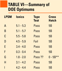
In looking at the optimum results recorded from each group, it is clear
that the interactive mask performance can be improved in general terms.
Mask G again gave bad results across all the tests that used pumice. Table
VI summarizes some of the more optimal data drawn from the DOE (tin plated
coupons only). This shows that the mask integrity can be improved and
the ionic levels maintained below the maximum 6.5µgs/inch2 (NaCl
equiv.) that is called out on the Bellcore 78 specs.
 |
Immersion
Tin Rework Procedures
One benefit of immersion tin comes from its ease of stripping in standard
tin-lead strippers. The panels can then be easily re-plated using the
standard process. Although first time tin coverage is normally good, this
assumes that the preclean and particularly the solder mask development
are good to avoid residues.
Re-work must be done carefully for two reasons: 1) The re-processing and
additional micro-etching of the base material may adversely affect the
edge lift on the mask; or 2) The re-work itself will result in further
loss of copper (etch + tin displacement) and hence minimum copper thicknesses
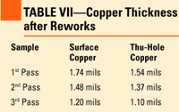
in holes will need to be carefully monitored. The described process has
been evaluated for copper loss during re-work and the results are shown
in Table VII. (Note: The etch rate through the cleaner and micro-etch,
37 microinches/min, and through the bifluoride based solder stripper was
2.4 microinches/min).
With the increasing application of immersion tin, much more practical
know-how has
developed.
This has been necessary to ensure the consistency and reliability of the
end finish and facilitate a smoother integration of the technology into
a volume production operation. The interactivity of the process with many
of the PWB materials is a key issue, and it is clear that more work will
be needed as the PWB industry continues on its perpetual trend of change
and improvement.
 |
The
immersion process has been shown to work effectively in both vertical
dip and horizontal conveyor modes. Both the vertical and horizontal processes
are capable of plating small and higher aspect ratio holes. Through holes
should be either plated fully open and plugged with a UV cure material
(preferable), or be fully and carefully plugged prior to plating to ensure
that there are no voids to trap chemistry. In dip mode, good precleaning
and rinsing are key, and a vibrator may be required for tiny, high aspect
ratio holes (to remove air). Board drying, (particularly the holes) is
also critical and should be done horizontally. Boards left with residual
traces of moisture may well have poor solderability and/or may experience
corrosion problems during storage and transit.
X-ray fluorescence spectrometry facilitates a convenient and effective
way to measure thickness.
Solderability testing after stressing (artificial aging) must be agreed
between supplier and customer and carefully applied and controlled. The
SERA technique for testing solderability is under longer-term investigation
and not enough results have been established to make a real determination
of its potential as a control tool. However, the method is in use by some
companies to evaluate the performance of immersion tin in production.
In terms of process integration any extensive baking should be carried
out before plating, or if not possible, should be avoided. When plating
gold tabs, a gold first operation covered with a peelable resist is preferred.
LPSM compatibility and/or dialing-in is key for optimizing ionics and
mask integrity. LPSMs over light pumice scrubbing although heavy pumice
footprints are better. Standard chemical pre-clean is inadequate for many
LPSM.
As originally published in the SMTA 2000 Conference Proceedings.
|
References |
Serving the Finishing
Industries. Since 1936.
PFONLINE and all contents are properties
of Gardner Publications, Inc.
All Rights Reserved.